
What Is a Semiconductor?
Explore the fundamental principles of semiconductors and the evolution from transistors to integrated circuits, and discover why semiconductor domain knowledge is essential for CS and AI engineers.

What Is a Semiconductor?
When most computer science (CS) engineers first hear the word "semiconductor," they think, "Oh, it's something used to make chips." That's not wrong, but it's not entirely accurate either. A semiconductor is literally a material that conducts electricity somewhere between a conductor and an insulator.
Materials can generally be classified into two categories:
- Conductors: Materials that allow electricity to flow easily, such as copper and aluminum.
- Insulators: Materials that resist the flow of electricity, such as glass and rubber.
Semiconductors fall somewhere in between.
Pure silicon (Si) conducts very little electricity at room temperature. However, by adding a small amount of impurities—a process called doping—we can control whether electricity flows through the material.
For programmers, a familiar analogy would be to think of a semiconductor as a hardware-level if statement.
Depending on a condition (voltage), current either flows (True) or does not flow (False).
This simple switching behavior forms the foundation of all digital computing.
Why Silicon?
Silicon belongs to Group 14 of the periodic table and is the second most abundant element in Earth's crust after oxygen.
It can be extracted from silica (SiO₂), which is commonly found in sand, making its raw materials widely available.
Alternative semiconductor materials, such as germanium (Ge) and gallium arsenide (GaAs), also exist.
However, silicon has one decisive advantage: it can form a stable silicon dioxide (SiO₂) layer through oxidation.
This oxide layer can serve as an electrical insulator, including the gate dielectric in transistors.
This property played a crucial role in making silicon the dominant material in the semiconductor industry.
Transistors: The Switches That Create 0s and 1s
If you studied computer science, you probably learned about logic gates such as AND, OR, and NOT.
The physical devices that make these logic gates possible are called transistors.
MOSFET Structure
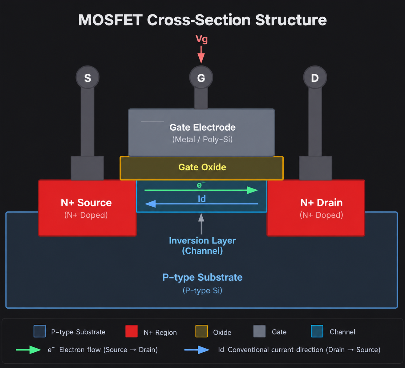
Most transistors used in modern digital semiconductor circuits are MOSFETs (Metal-Oxide-Semiconductor Field-Effect Transistors).
Their basic structure is surprisingly simple:
- Source: The region from which charge carriers originate. As the name suggests, it is the "source" of carriers.
- Drain: The region through which charge carriers leave the transistor.
- Gate: The control terminal that regulates current flow by applying voltage.
- Channel: The path through which charge carriers move between the source and drain.
- Gate Oxide: A thin insulating layer separating the gate from the channel.
💡 Why are they called "Source" and "Drain"?
These names refer to the movement of charge carriers. The source supplies carriers, while the drain collects them.
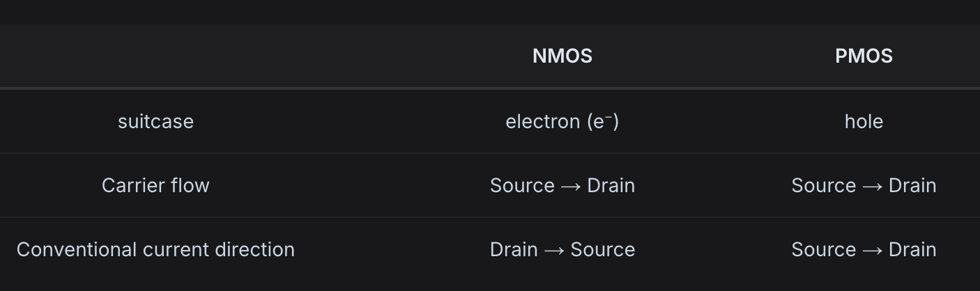
Conventional current (I) flows in the opposite direction to electron movement. Therefore, in an NMOS transistor, conventional current flows from the drain to the source.
This may seem confusing at first, but a useful way to remember it is that electrons generally enter the NMOS channel from the source.
When voltage is applied to the gate, charge carriers accumulate in the channel, allowing current to flow (ON = 1).
When the gate voltage is removed or reduced below the required level, the channel stops conducting significant current (OFF = 0).
That's the basic principle.
Everything you learned in computer science—operating systems, networking, deep learning, and more—ultimately runs on billions of these tiny switches turning on and off billions of times per second.
💡 There is no such thing as a perfectly ON or OFF transistor.
Even when a transistor is turned OFF, a very small amount of current can still flow.
This is called leakage current.
In other words, 0 and 1 are not strictly defined by whether current flows at all. Instead, they are determined by whether the electrical signal exceeds or falls below a certain threshold.
As semiconductor technology scales to smaller process nodes, controlling leakage current becomes increasingly challenging. Leakage can contribute significantly to power consumption and heat generation, particularly in advanced technology nodes.
In certain designs and operating conditions, leakage power can account for a substantial portion of total chip power consumption.
This is one reason semiconductor manufacturers have continuously evolved transistor architectures—from planar transistors to FinFETs and, more recently, Gate-All-Around (GAA) transistors.
N-Type and P-Type Semiconductors
Depending on the type of impurity used for doping, semiconductors can be classified into two categories.
- N-type: Created by adding donor impurities such as phosphorus (P) or arsenic (As), resulting in electrons being the majority charge carriers. The "N" stands for "Negative."
- P-type: Created by adding acceptor impurities such as boron (B), resulting in holes (the absence of electrons) being the majority charge carriers. The "P" stands for "Positive."
When N-type and P-type semiconductor regions form a junction, they create a PN junction, which is the foundation of a diode.
By combining appropriately doped regions with additional structures, transistors can be constructed.
CMOS (Complementary Metal-Oxide-Semiconductor) technology combines N-channel MOSFETs (NMOS) and P-channel MOSFETs (PMOS) in a complementary configuration to implement logic gates.
This approach dramatically reduces static power consumption.
As a result, nearly all modern digital integrated circuits are based on CMOS technology.
From Transistors to Chips: The Journey of Integration
The Birth of the Integrated Circuit (IC)
In 1958, Jack Kilby of Texas Instruments developed an integrated circuit (IC) that connected multiple electronic components on a single semiconductor substrate.
Before integrated circuits, transistors, resistors, and capacitors were manufactured as separate components and connected using wires.
The integrated circuit revolutionized electronics by integrating these components onto a single chip.
For computer science engineers, consider the following analogy.
Connecting individual electronic components with wires resembles a microservices architecture, where separate services communicate over a network.
An integrated circuit is somewhat like moving toward a monolithic architecture.
By integrating components onto a single substrate, communication distances become shorter, system size decreases, and reliability improves.
The Explosive Growth of Transistor Density
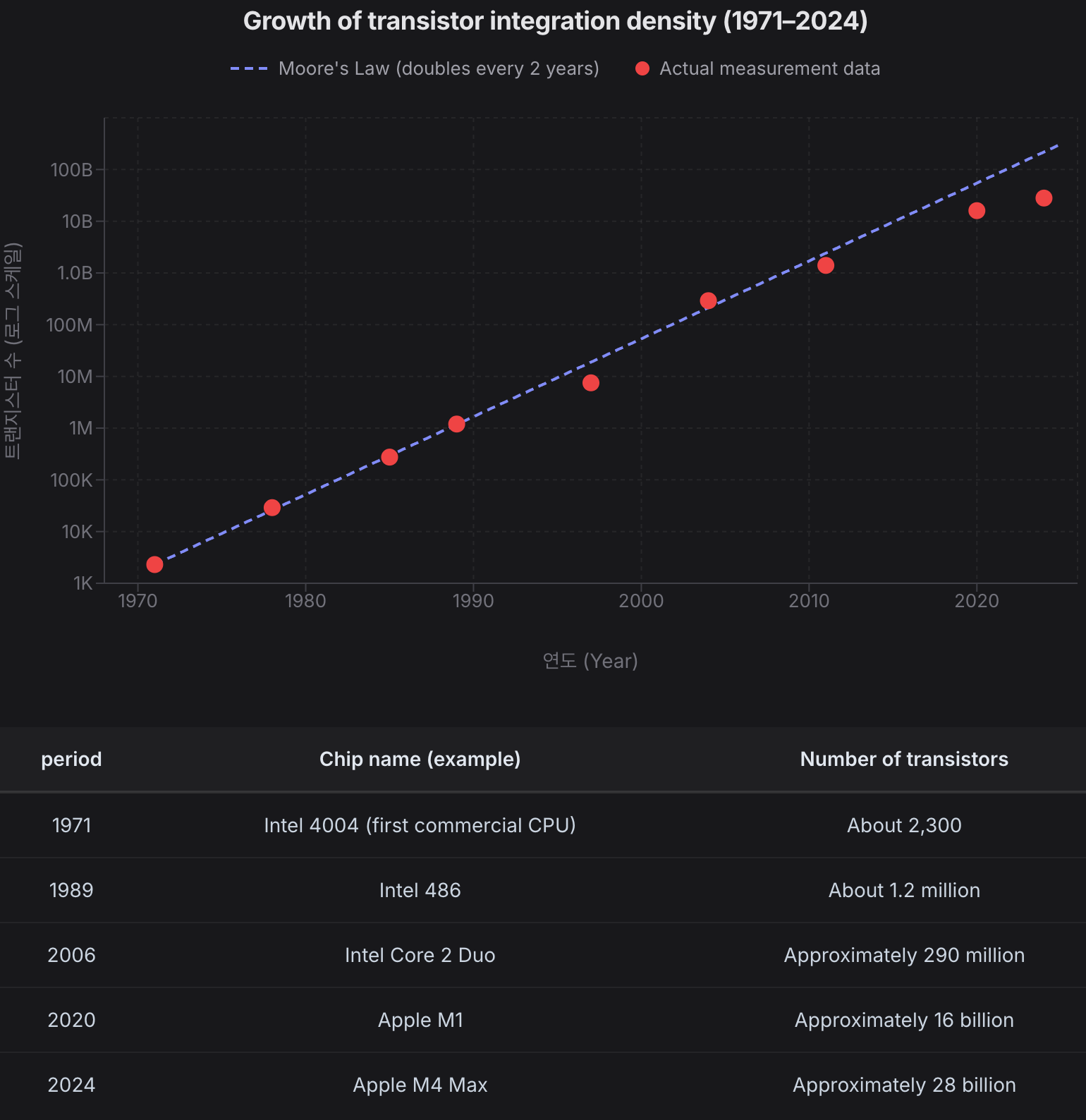
Over the past 50 years, the number of transistors integrated into a single chip has increased by more than ten million times.
How was this possible?
The answer lies in the continuous advancement of technologies that allow transistors to become smaller and smaller.
One of the most important technologies enabling this progress is photolithography.
And that is the central topic of this blog.
How a Chip Is Manufactured
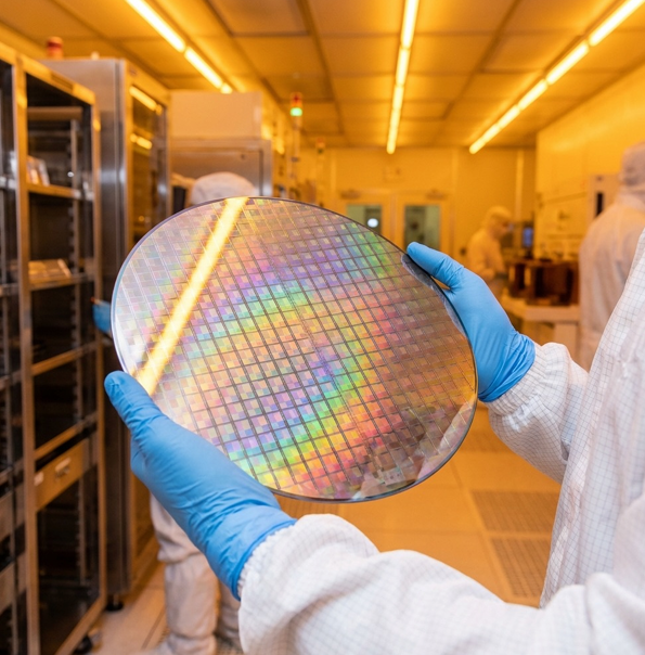
Manufacturing a single semiconductor chip requires hundreds of processing steps.
At a high level, the manufacturing process can be summarized as follows:
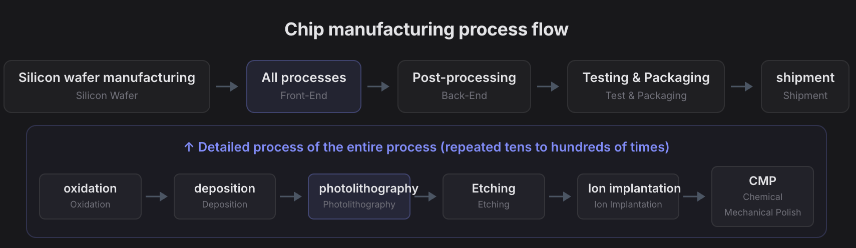
Among these processes, photolithography is responsible for transferring circuit patterns onto silicon wafers.
It is one of the most critical and expensive steps in semiconductor manufacturing.
In advanced semiconductor fabrication, lithography-related operations can account for a significant portion of total manufacturing costs and process complexity.
Depending on the technology node and process flow, lithography may represent approximately 30–35% of manufacturing costs and a substantial share of repeated processing operations.
Producing a chip at an advanced 5 nm-class technology node may require more than 80 lithography steps.
Why Does This Matter to AI Engineers?
You might reasonably ask:
"I'm a software engineer. Why do I need to understand transistor structures?"
The answer is simple:
To work with semiconductor manufacturing data, you need to understand where that data comes from and why it is generated.
The SMILE platform analyzes semiconductor manufacturing data, including data generated during photolithography processes.
Examples include:
- Overlay: Misalignment between circuit patterns on different layers.
- Critical Dimension (CD): The measured width or size of a critical circuit feature.
- Defect Data: Information about manufacturing defects and abnormalities.
These measurements are closely connected to the physical behavior of semiconductor manufacturing processes.
Without understanding their physical meaning, AI engineers may encounter several problems:
- They may create feature combinations that make little sense from a semiconductor physics perspective.
- They may fail to distinguish actual process defects from measurement noise.
- They may develop models with high statistical accuracy that nevertheless produce results process engineers cannot trust.
This leads to an important distinction.
Domain knowledge does not simply determine how accurately an AI model performs. It determines whether that AI model can actually be used in a real manufacturing environment.
A model may achieve excellent benchmark results, but if its predictions contradict known process behavior or cannot be explained to engineers, it will struggle to gain acceptance on the fab floor.
This is particularly important in semiconductor manufacturing, where process decisions can affect expensive equipment, production throughput, and product yield.
The purpose of this blog is to provide AI and software engineers with the essential semiconductor domain knowledge they need—through the shortest and most practical learning path possible.
Key Takeaways
-
Semiconductor: A material whose electrical conductivity can be controlled through factors such as doping and electric fields. Think of it as the physical foundation of a hardware-level if statement.
-
Transistor (MOSFET): An electronic switch controlled by gate voltage. It forms the foundation of modern digital computing.
-
CMOS: A complementary combination of NMOS and PMOS transistors. The standard technology for low-power digital circuits.
-
Integrated Circuit (IC): A chip that integrates billions of transistors and other electronic components onto a single semiconductor substrate.
-
Photolithography: A critical manufacturing process that enables the creation of increasingly complex and densely integrated semiconductor circuits.
Photolithography is where semiconductor physics, precision engineering, and advanced manufacturing meet—and it will be the main focus of this blog.